We provide efficient and high-quality turnkey PCB assembly service to our customer. In order to achieve the fastest possible turnaround of the highest quality product, we continuously strive to improve our services and to make each step as efficient as possible. One of the most important factors in the overall efficiency of each PCB assembly project is the client’s understanding of PCB assembly process. This page provides an overview of some standard but important turnkey PCB assembly process. Generally, we can provide the following steps for our clients:
1: Component Purchasing
We have a professional expert for component purchasing from reliable sources in high quality and reasonable price which can guarantee the buying process
Therefore, we can reliably supply the parts you need even rare and hard to find parts.
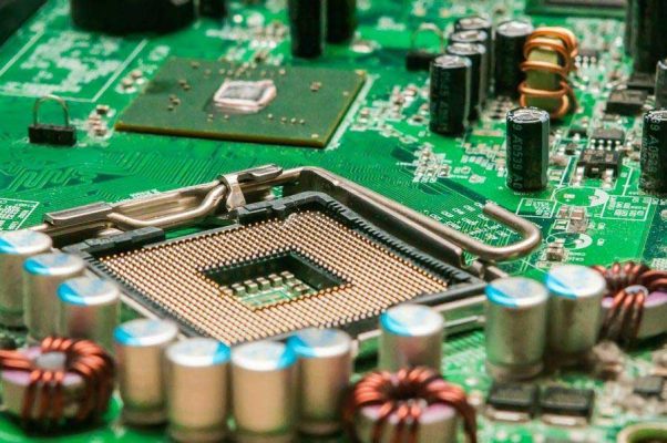
2: Quality Control of Components
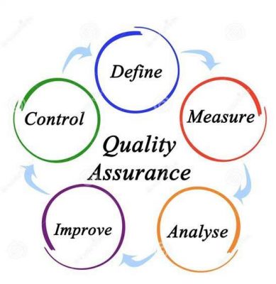
We also apply a standard quality control tests and techniques in purchasing components in order provide best services for our clients along with cooperation with professional team of experts and electronic engineers.
3: Solder Paste Printing
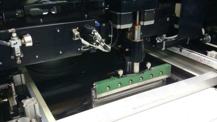
Solder paste (or solder cream) is a material used in the manufacture of printed circuit boards to connect surface mount components to pads on the board. Before soldering, all PCB boards should print solder paste so that the components can be soldered by pick & place machine.
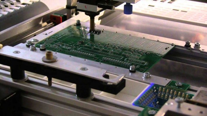
4: Pick & Place SMD Parts
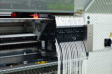
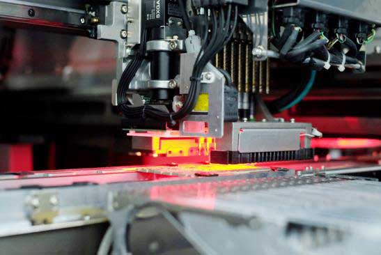
Once bare PCBs printed solder paste, they are moved to automated Pick & Place machines for the actual mounting of components on their associated pads. Part placement is 100% machine automated for maximum accuracy and efficiency, and uses the project’s Centroid file for component coordinates and rotation data. The boards are again inspected after components have been mounted to ensure all placements are accurate before the soldering process begins.
This stage might need to be performed multiple times, depending upon the specifics of a given project. Double-sided SMT boards require one round of placement for the top and one for the bottom, and projects requiring wave soldering due to a high number of through-hole parts will normally have their components machine-placed as well.
5: Reflow Soldering
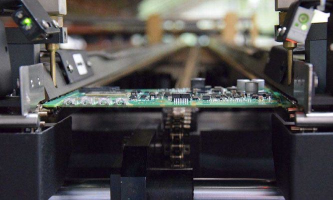
With parts mounted securely in place with solder paste underneath their pads, it is time for the PCBs to enter the reflow soldering oven. This is the most common method for PCB assembly in the industry today since it is much more flexible in terms of PCB layout requirements compared with wave or hand soldering. Most of the time, we can use reflow soldering for a majority of the parts on a board, and then pass the mostly-assembled boards to our highly skilled hand soldering team for the final few connectors and through hole components. We have more than 6 reflow oven in its plant.
For double-sided assembly projects, the boards will need to be reflowed once for each side. A special adhesive is applied underneath the components that were soldered in the first run to prevent them from detaching and falling off the board when their solder is re-heated.
6: Wave soldering
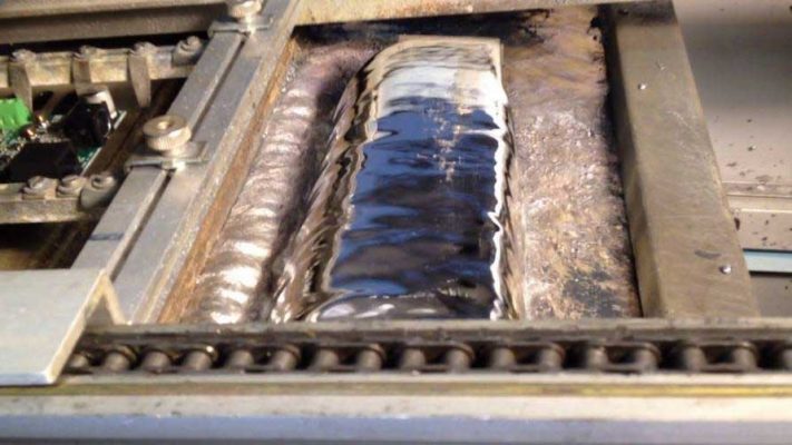
Wave soldering is a large-scale soldering process by which electronic components are soldered to a printed circuit board (PCB) to form an electronic assembly. The name is derived from the use of waves of molten solder to attach metal components to the PCB. It is for Through hole components soldering. Normally if your order is small, it will not be soldered by wave soldering machine. If you insist, extra fee will be added.
7: THT Components Placement
Through-hole-technology (THT) involves inserting leads of components into drilled holes in the PCB. Leads can then be soldered onto pads or lands on the solder side of the board, usually with a simple soldering iron by hand or wave soldering process. Soldering a Dual-in-line package (DIP) IC on the PCB is an example of THT.
8: Pick & Place SMD Parts
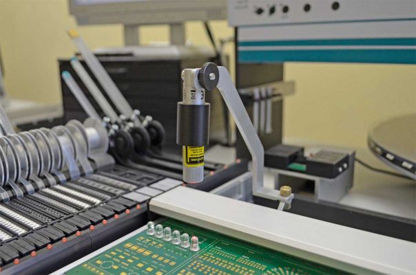
An import step in the assembly process is placing the components on the board and for Surface Mount Devices (SMD) this is done with an automated Pick & Place machine. Using automated Pick & Place machines is much faster and more accurate than a manually placement of the surface mount components. Such machine has automated registration and super-fast component placement with built in checks that use a variety of cameras.
9: Flipping
We have novel flipping machines that handle this step.
10: AOI Checking/X-Ray
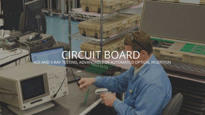
After a reflow oven process, any boards including BGA, QFN, or other lead-less package types are sent for X-Ray Inspection. Designed for heavy production environments, X-ray is used to inspect raw PCBs and assembled PCBs containing advanced components such as BGAs, uBGAs and Flip Chips. This versatile system features patented, award-winning X-ray camera technology that generates high-resolution, high-sensitivity images, revealing defects as small as 0.001 inches with a full one-inch diameter field of view. X-ray inspection is often paired with the electrical testing provided by ICT or functional test. It is an ideal low-cost solution for verifying prototypes as well as complex boards in volume production.
Automated X-ray inspection is based on the same fundamental ideas as AOI, but as opposed to using normal visible light to inspect the outside of the PCB, X-ray inspection can find faults that would otherwise be hidden from view. The X-ray inspection machine produces images of the PCB which are then analyzed by image processing software, which can detect abnormalities and the presence or absence of features like components or wiring. This is especially important because it means that X-ray testing finds faults that AOI cannot. If implemented during the manufacturing process, this can save a significant number of resources because it immediately prevents defective parts from wasting any further time during assembly.
X-ray testing is useful not just during manufacturing, but during rework. As part of the standard reworking and repair process, WORLD engineers scan returned PCBs using the X-ray testing machine to efficiently determine the faulty connection or component causing the PCB to fail. This can normally be done quickly since the X-ray inspection machine can be geared either for low- to medium-volume production runs, or the inspection of just a few damaged PCBs. The reworking procedure is therefore kept as short as possible, far shorter than it would be where our engineers to rely on regular visual inspection.
11: Visual Inspection (Repairing)
Testing of the PCBs in design and manufacturing is crucial for quality control. Companies want to avoid realizing the product is faulty when it is already in the production or in the market. There is always chance for defects even after following the proper design and production processes. Identifying the defects before manufacturing the final product is essential for ensuring performance, reliability, and functionality of the products. Errors in PCB assemblies may occur due to human error, wrong production processes, and poor design. Luckily, with the help of proper testing procedures and inspection measures the quality and the reliability of the product can be maintained.
The benefits of a PCB assembly visual inspection include;
- Paying attention to preventative measures instead of addressing the issue after the production.
- Using preventative measures are helpful since fixing the problems on a finished product is costly and time consuming.
- Identifying and addressing errors such as short circuits, and functional issues.
- Reducing the number of waste and cost since PCB assembly testing requires a small-scale assembly and a prototype rather than the complete product.
PCBs can be found in different shapes, sizes, and quality requirements. They are also consisted of different components. Each part has an impact on the overall performance of the PCB and the assembly as a whole. Therefore, it is crucial to inspect every part of the PCB assembly such as electrical conductivity, mechanical strength, quality of the hole wall, cleanliness, and component placement.
Visual inspection is the most basic form of an inspection. This is basically a tech review checking things like wrong or missing components, solder bridges, missing solder, tombstoning and different kinds of errors. This method is dependent on the operator therefore it may be time consuming when large amounts of PCBs are needed to check.
12: Technical Test and Control of Circuits
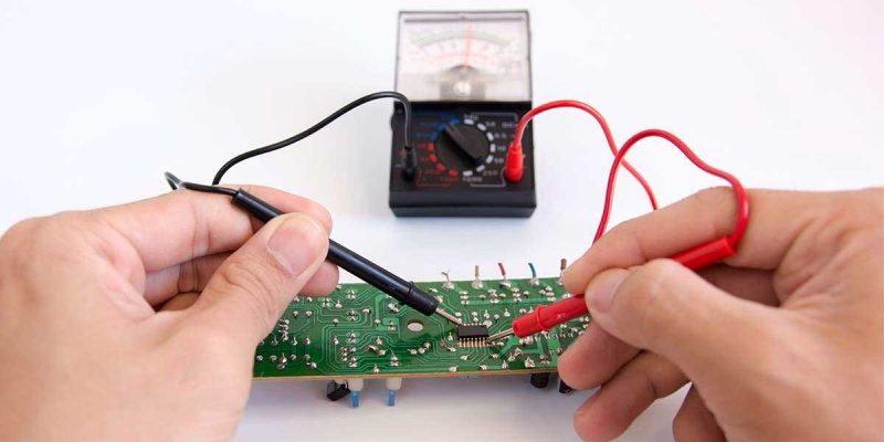
When you order printed circuit boards (PCB), you know the pricey consequence of failure. The last thing you need financially is for your PCBs to suddenly drop dead — or to have a shortened life span because of a design or QA issue. PCB assembly testing methods are an integral part of the manufacturing process. Reputable electronics contract manufacturers (ECMs) offer a variety of PCB testing methods, enough that sometimes it’s hard to keep them straight.
13: QC/Package
For PCB packaging, you draw the schematic, load the components of the schematic, which are the pads on the PCB, and then after the conversion is completed, the package connection is completed. Various parameters of actual electronic components, chips, etc. (such as component size, length and width, in-line, patch, pad size, pin length and width, pin spacing, etc.) are displayed graphically, so that it can be called when drawing a PCB diagram. Encapsulation is to combine abstracted data bai with behavior (or du function) to form an organic whole. PCB packaging is the actual electronic components, chips, and other parameters expressed through the use of graphics, so that they can be called when drawing the PCB diagram. It is also the size of the pad on the board when the component is soldered to the PCB.
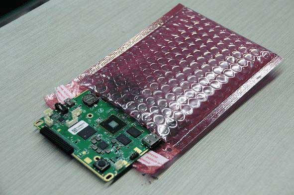
14: Delivery
We have access to forwarders in order to send the items to anywhere on the planet with a door-to-door system and we can guarantee the process.

